SK Hynix to Boost SSD Performance with Over 100 Specialized Processors
The new H-TPU architecture replaces traditional controllers with specialized cores to improve efficiency.
A New Approach to Data Management
Memory manufacturing giant SK Hynix is planning a major technological shift. The company has introduced the H-TPU (Hynix Transaction Processing Unit) architecture, which radically changes how SSD controllers operate. Instead of relying on traditional, general-purpose processors, the company intends to use over a hundred compact, specialized cores to streamline the data transfer process.
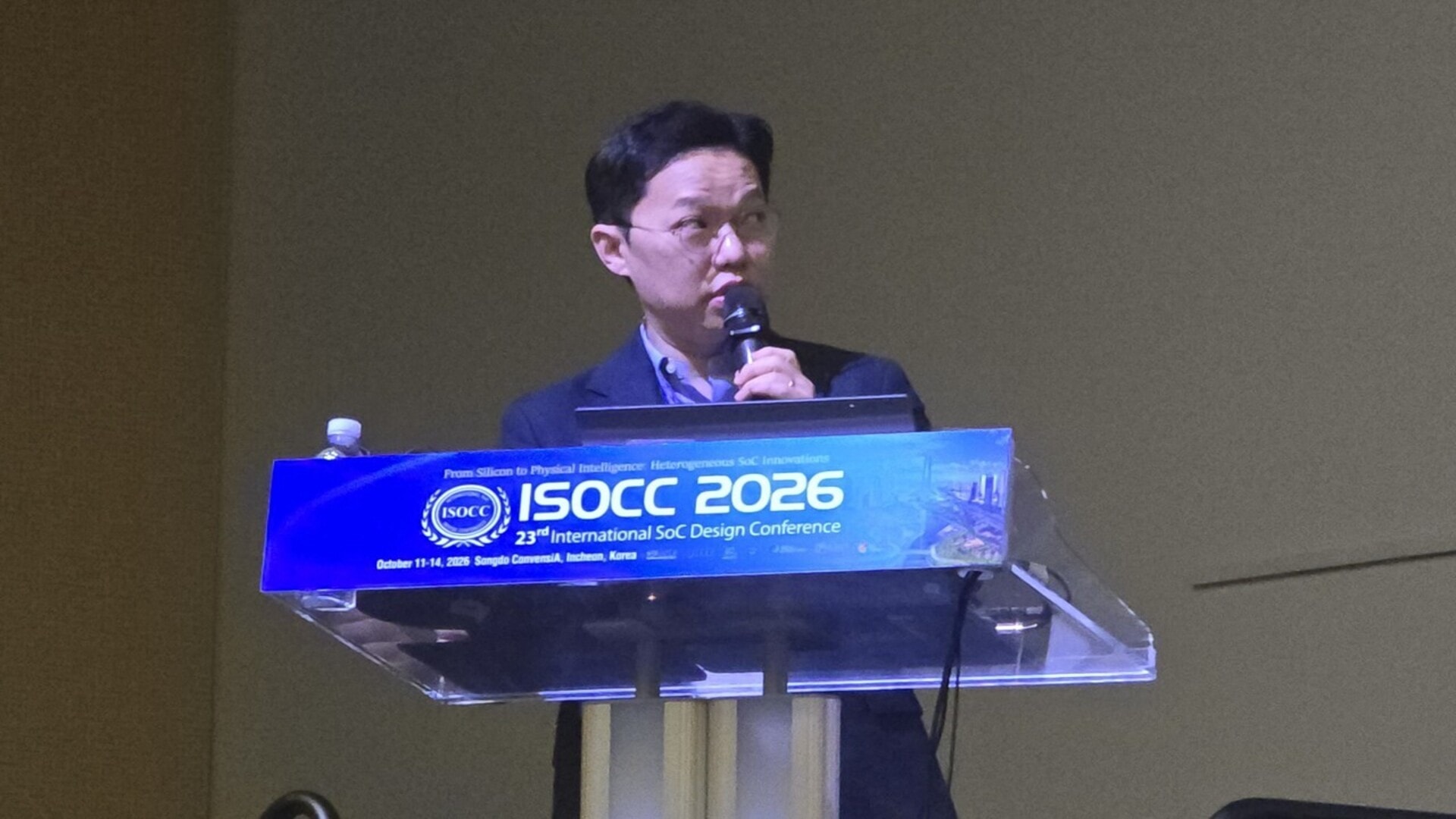
Speaking at the International SoC Design Conference, SK Hynix Vice President Koo In-jae noted that modern SSD controllers are reaching their performance limits. As data transfer speeds increase, existing processors consume more power and occupy more space on the chip, creating a significant challenge for the industry.
How H-TPU Technology Works
SK Hynix’s H-TPUs are designed to handle routine and repetitive operations, such as managing input/output (I/O) paths. The primary advantage of these specialized cores is their small footprint: each occupies only 4% of the area of a standard processor core and consumes just 2.5% of its power.
The architecture utilizes a four-stage pipeline and sequential execution, which is ideal for memory systems. Importantly, the controller does not activate all processors simultaneously; the system engages only as needed, while the remaining cores remain in standby mode. Meanwhile, the main processor continues to handle complex tasks, such as error correction and data security policy enforcement.
The Future: AI and PCIe 8.0 Standards
This technology is directly linked to the growing demands of artificial intelligence. SK Hynix plans to integrate H-TPUs into its 'Storage Next' architecture, which is optimized for processing small data packets. This is particularly important for modern AI models, which frequently work with transactions as small as 512 bytes—only one-eighth of the traditional 4KB standard.
SK Hynix aims to incorporate this innovation into next-generation enterprise SSDs and High Bandwidth Flash (HBF) memory. This will become especially relevant as PCIe 6.0, 7.0, and 8.0 interfaces become widespread, further increasing data transfer speeds. While specific commercial timelines have not yet been announced, this move by SK Hynix demonstrates that the memory industry is actively preparing for a new, more efficient era of data processing.